
调控碳化硅陶瓷的电阻率,实现其在功率电阻器中应用
多孔碳化硅 (SiC) 基陶瓷因其出色的结构(例如,出色的化学、机械和热稳定性)和功能(例如,受控的电阻率)特性而广泛用于许多具有技术重要性的应用中。各种先进应用都需要具有可控电阻率的多孔 SiC,例如电力电子设备、半导体加工部件、聚变反应堆、热电能量转换、电磁屏蔽和可加热过滤器等环境应用。烧结多孔碳化硅的电性能受其化学成分、加工条件和微观结构的影响很大。本文回顾了某些关键因素的影响,例如多型、掺杂条件、孔隙率 (%)、添加剂成分(氧化物添加剂、元素添加剂、金属氮化物/碳化物添加剂等)和多孔SiC电阻率的加工条件。
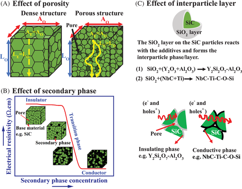
FIGURE 1 Schematic diagram to represent the effect of the (A) porosity, (B) conductive phase addition, and (C) interparticle layer, on the electrical resistivity of porous SiC. In (A), AO and LO are the cross-sectional area and length of the bulk material, respectively, while AE and LE are the effective cross-sectional area and length of the porous material, respectively
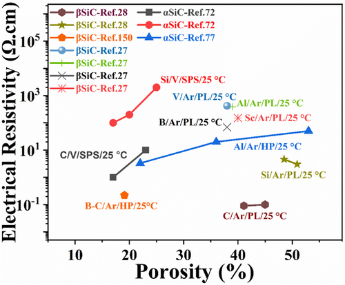
Effects of nitride/carbide additives on the electrical resistivity of porous SiC ceramics sintered in different atmospheres (N, Ar, V: vacuum) and sintering techniques (PL: pressureless, HP: hot-pressed). The labels of the data points are in the order: additive/sintering atmosphere/sintering technique/measurement temperature
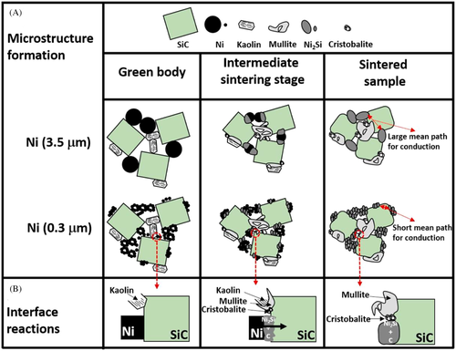
Effect of reducing the Ni particle size from 3.5 to 0.3 μm: (A) microstructure formation and (B) interface reactions, with SiC particle size = 4.5 μm and kaolin particle size = 2.1 μm
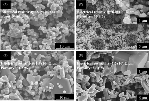
Fracture surfaces of porous SiC ceramics with controlled electrical resistivity and porosity (%) sintered at 2000°C with the initial SiC particle size of 0.5 μm; (A) N-doped (reproduced with permission from Ref. [27] 2021 Elsevier), (B) Sc-doped (reproduced with permission from Ref. [27] 2021 Elsevier), (C) boron nitride-doped (BN-doped) sintered in nitrogen (reproduced with permission from Ref. [30] 2021 Elsevier), and (D) BN-doped sintered in argon (reproduced with permission from Ref. [30] 2021 Elsevier)